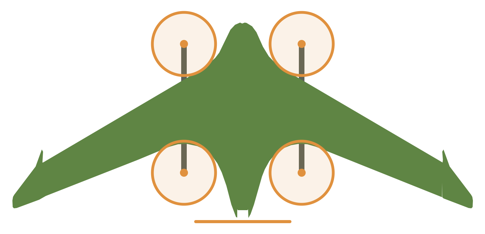
Charge Node: power stage
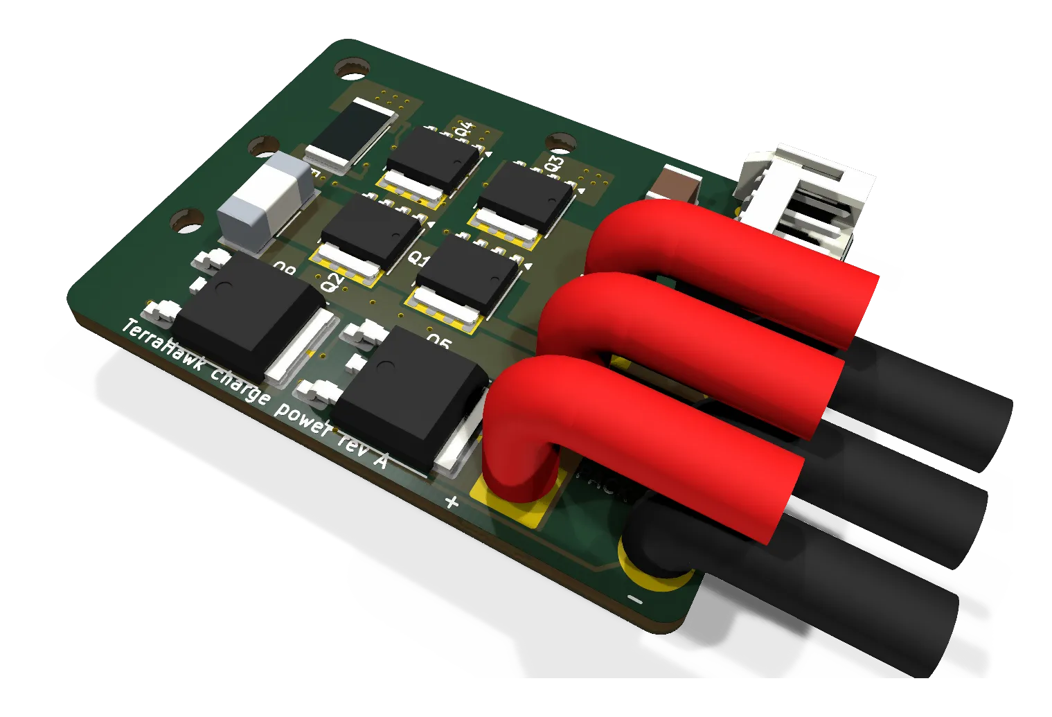
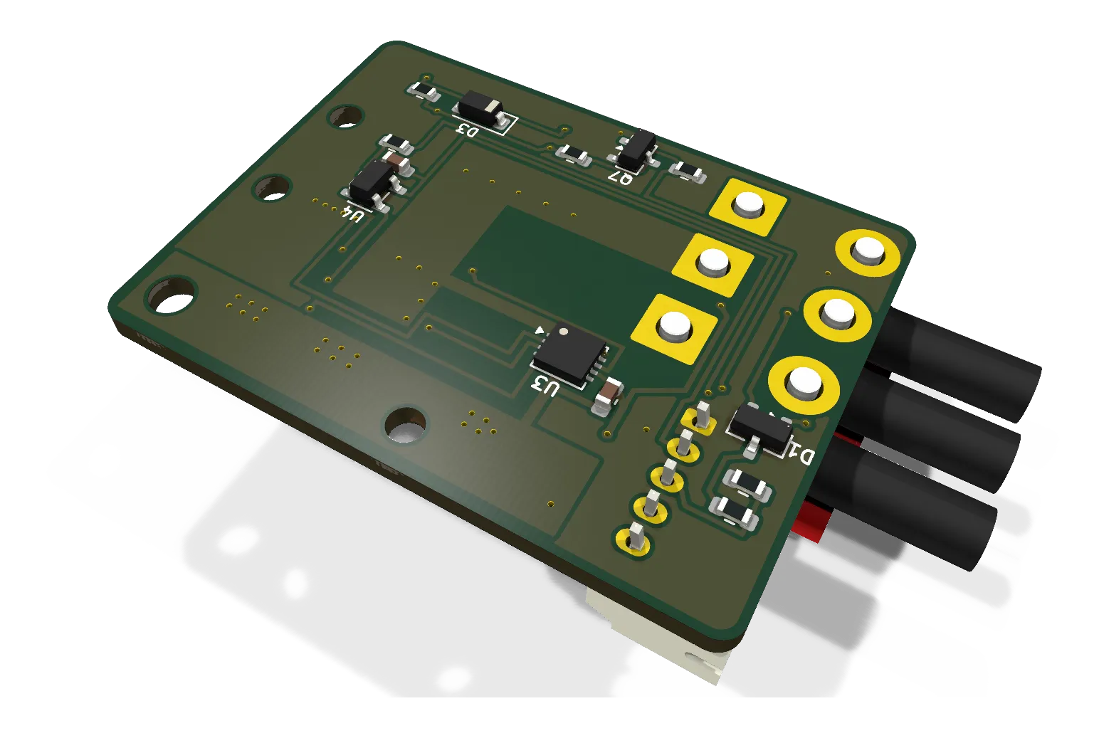
Boards / Charge node power stage on 2 oz copper: LT4320 ideal-diode bridge, fuse, load switch and current shunt.
The power stage carries the charge current from the keel charge plates to the pack, through a bridge, a fuse, a switch and a shunt.
- Revision
- A rc6
- Sheets
- 2
- Parts
- 32
- Board
- 40 × 30 mm
- Copper layers
- 2
- Footprints
- 32
- Location
- aircraft
- Bus
- none: a 5-wire link to the sense board
- Status
- Rev A rc6: routed, DRC clean
What it does
The power stage is one of the two boards of the charge node. The other is the sense board. The charge node schematic shows the two as one circuit, for review. The power stage has no MCU. The sense board reads it and controls it over the link.
An LT4320 ideal-diode bridge lets either plate polarity charge the pack. With no plate voltage, the pack cannot reach the plates. A 10 A fuse opens only on a hard fault. The charge-enable switch is two P-channel MOSFETs back to back, so when it is off no current flows in either direction. It stays off when the node is off, in reset or unplugged. A 5 mΩ shunt gives 0.25 V per A. A BAV70 diode-OR reads the plate voltage, about 0.7 V low.
Where it sits
The board is 40 x 30 mm and 12 mm high. It stands on its 40 mm edge in the starboard pocket of the battery bay, beside the pack. The PETG Charge Power Bracket on the starboard wall holds it on four M2 heat-set inserts. A zip-tie tunnel on the bracket holds the pigtails, so cable pull does not reach the solder joints.
Main parts
| Part | Function |
|---|---|
| LT4320IDD | Ideal-diode bridge controller, 9 to 72 V |
| 4 x PSMN7R0-60YS | Bridge MOSFETs |
| NANO2 10 A | Fuse, not field-replaceable |
| 2 x SUD50P06-15L | Charge-enable switch |
| 2N7002, BZT52C12 | Gate driver, 12 V gate clamp |
| 5 mΩ 2512, INA180A2 | Shunt and amplifier, 50 V/V |
| BAV70 | Plate voltage sense |
Connections
| Connector | Type | To |
|---|---|---|
| J4, J5 | XT30 male pigtail, 16 AWG | Charge plate leads, one for each side |
| J6 | XT30 male pigtail, 16 AWG | Pack tap off the main feed |
| J15 | JST-PH 5-pin | Link to the sense board J14 |
The board pads are dead when unplugged, so the board carries the male XT30s.
Status
Rev A rc6, frozen on 2026-09-29. The board has two copper layers of 2 oz, for the 10 A return. It is routed, and DRC gives 0 errors. th-avionics approved it.
CAUTION: Do not build a power stage from rc1 to rc3. Their LT4320 bottom gates are crossed the wrong way, which shorts the live input to the return. rc4 corrects it.
The first bench test uses a lab supply in place of the pad, with each polarity in turn.
Schematic and layout
The 3D board loads when you open this view.
Files
From the EDA repository at revision b201257 (2026-10-12). Open the files in KiCad 10 or later.
Comments
Comment on the whole page here, or on one section or step with the button beside it.