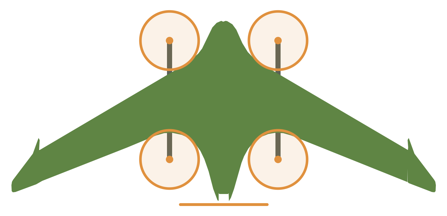
Charge Node: sense board
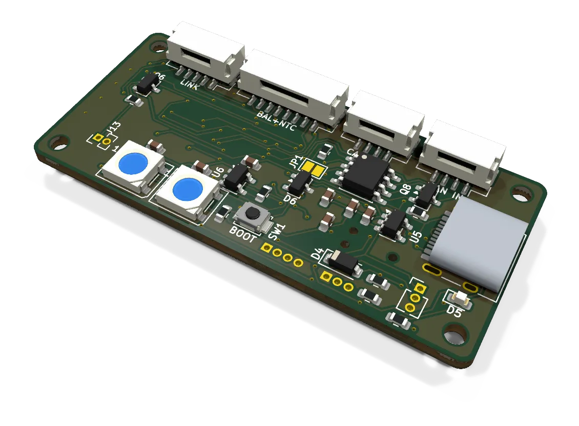
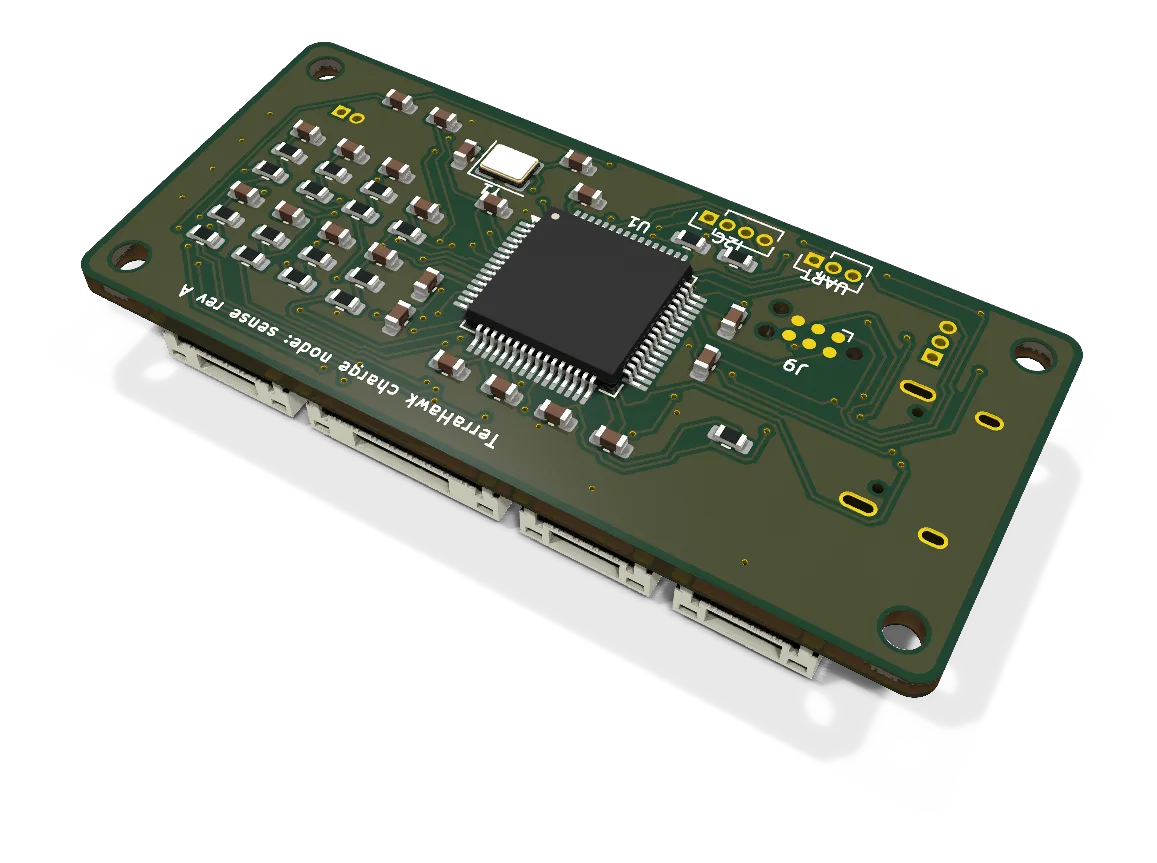
Boards / Charge node sense board: STM32 running AP_Periph, DroneCAN, cell and pack sensing, balancer switch.
The sense board reads the pack cells and temperature and connects the charge node to DroneCAN.
- Revision
- A rc6
- Sheets
- 4
- Parts
- 84
- Board
- 55 × 25 mm
- Copper layers
- 2
- Footprints
- 83
- Location
- aircraft
- Bus
- DroneCAN, aircraft CAN bus 2
- Status
- Rev A rc6: routed, DRC clean
What it does
The sense board is one of the two boards of the charge node. The other is the power stage. The charge node schematic shows the two as one circuit, for review.
The board holds the STM32F405 that runs AP_Periph, node 20 on CAN bus 2. It reads the six balance lead taps through 910 kΩ over 100 kΩ dividers at 0.1 %. The firmware scale is SCALE(10.1), so do not fit 900 kΩ parts. The pack voltage comes from the top tap, and a 10 kΩ NTC on the pack gives its temperature.
The power stage sends the plate voltage and the charge current over the link. The sense board sends CHARGE_EN back. It also switches the balancer negative lead (BAL_EN), and two WS2812B LEDs show status.
Where it sits
The board is 55 x 25 mm and 8 mm high. The last fit (Ryan, 2026-10-04) puts it flat on the floor under the FC deck, on the PETG Charge Sense Floor Tray. The GH plugs face starboard and the USB-C end faces aft. The SWD pads are on the back face, so program the board before you fit it.
On 2026-10-05 the 4-in-1 lift ESC moved to the same floor area. Do a check of this position again before you fit the node.
Main parts
| Part | Function |
|---|---|
| STM32F405RGT6 | MCU, runs AP_Periph |
| TJA1051T/3, NUP2105L | CAN transceiver and TVS |
| AP2112K-3.3 | 3.3 V LDO |
| AO3401A | Bus 5 V load switch, off while USB is present |
| 12 x 0.1 % resistors | Cell tap dividers |
| AO3400A | Balancer power switch |
| 2 x WS2812B | Status LEDs |
Connections
| Connector | Type | To |
|---|---|---|
| J1, J2 | JST-GH 4-pin | CAN bus 2 in and out |
| J3 | JST-GH 8-pin | Balance lead pins 1 to 7, NTC on pin 8 |
| J14 | JST-GH 5-pin | Link to the power stage J15 |
| J12 | USB-C | Bench power and first flash |
| J13 | 2 pads, 1.27 mm | Balancer negative lead |
| J8 | 3 pads, 1.27 mm | LED strip |
| J9, J10, J11 | Pads only | SWD, debug UART, spare I2C |
Status
Rev A rc6, frozen on 2026-09-29. The board has two copper layers of 1 oz. It is routed, and DRC gives 0 errors. A pre-order review on 2026-09-27 found nothing that blocks a build. On USB power alone the CAN supply is marginal, so feed 5 V on J1 for bench CAN.
Schematic and layout
The 3D board loads when you open this view.
Files
From the EDA repository at revision b201257 (2026-10-12). Open the files in KiCad 10 or later.
Comments
Comment on the whole page here, or on one section or step with the button beside it.