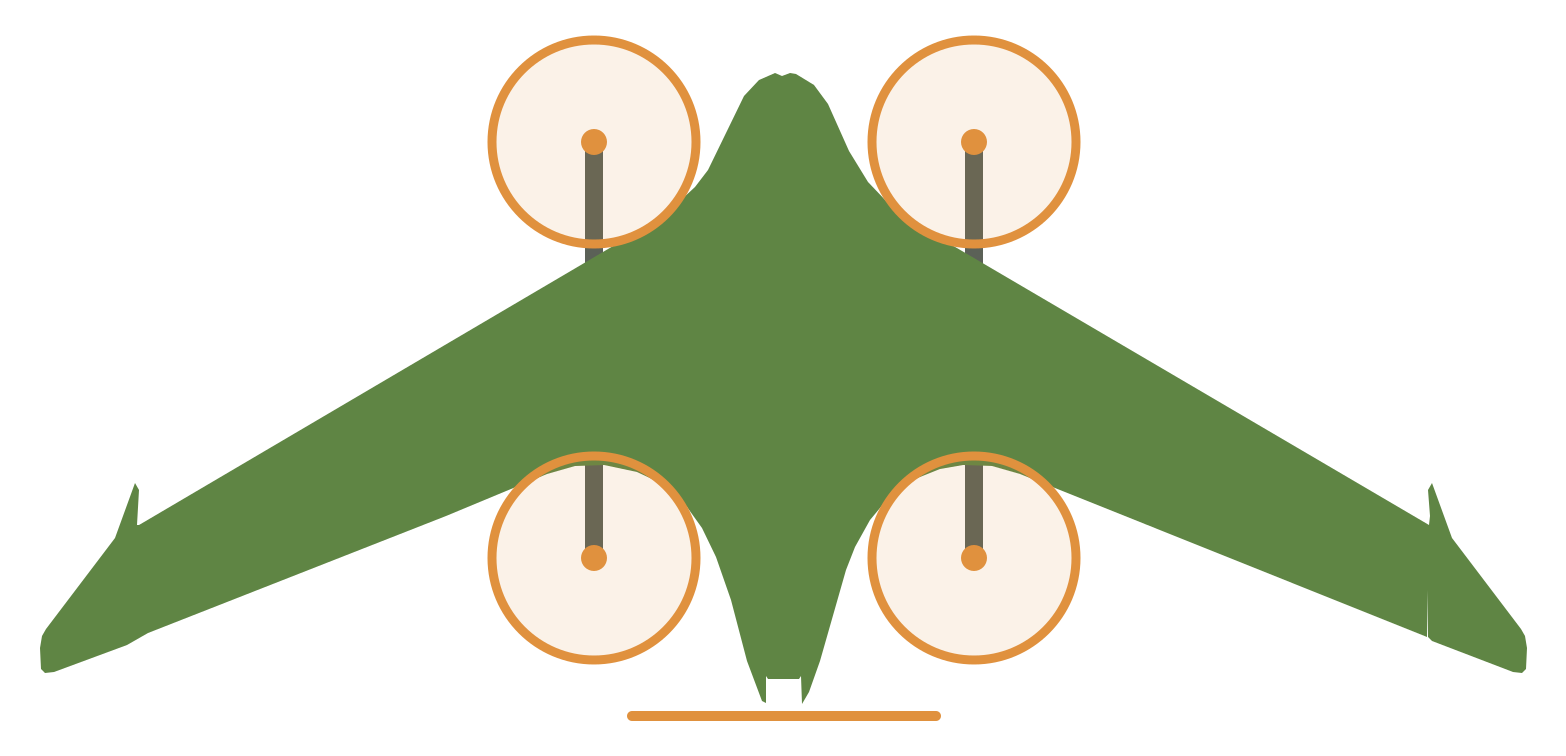
Lights node
Boards / DroneCAN, 2S lighting battery
The lights node drives the strobes and the landing light from its own 2S lighting battery, controls the position lights on a small sister board, guards the battery's charge from the dock, and supplies 5.2 V to the beacon.
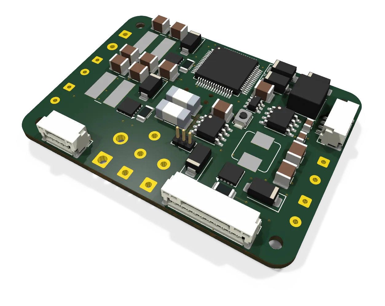
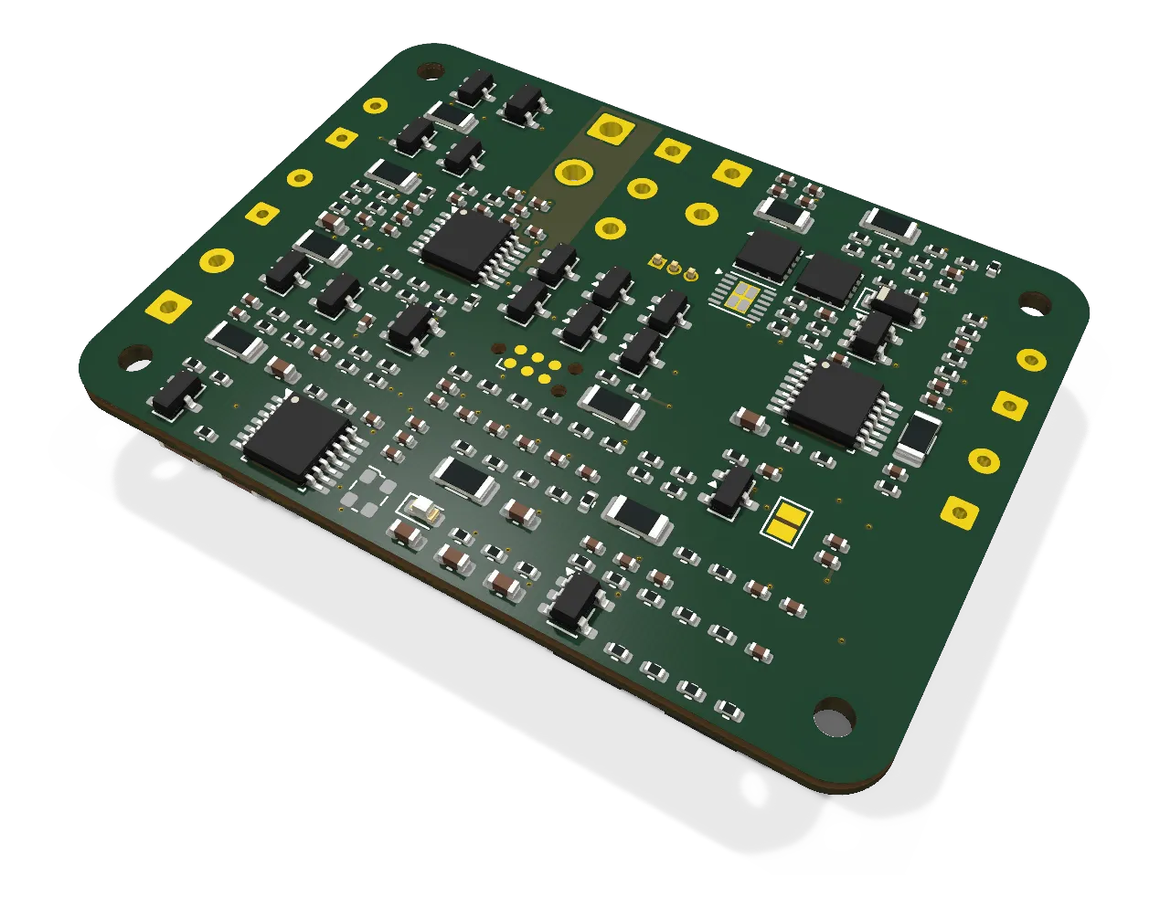
- Revision
- A draft
- Sheets
- 1
- Parts
- 226
- Board
- 55 × 40 mm
- Copper layers
- 4
- Footprints
- 230
- Location
- aircraft
- Bus
- DroneCAN, node id 70
- Status
- Rev A draft: 106 x 41 on edge in the starboard slot, six layers, fully routed, DRC clean (2026-10-17)
What it does
The lights node drives the strobes and the landing light, and controls the position lights. Each light has its own constant-current channel with brightness control. The lights use a 2S lighting battery, not the flight pack. The dock charges that battery through two contacts on the keels, and the node decides whether the charge may flow.
The node also supplies +5V_LIGHT (5.2 V) to the beacon, so this battery is the backup supply for the GPS and the radios. A P-MOSFET disconnect is closed by default. A TLV431 opens it in hardware below 6.03 V, so a crashed MCU cannot open the battery. The node reports the battery to the FC as BATT3.
Since 2026-10-11 the three position-light channels are on the position-light driver, and the lighting battery is charged by the dock, not on board. An on-board charger made about 2 W next to the LiPo with nowhere to shed it, so it was dropped (the lights charger board is withdrawn).
The dock’s isolated 2S supply reaches the node through the aft segments of the two keel strips, L+ on the port keel and L- on the starboard keel, and charges at 0.65 A to 8.40 V, reading the cell voltages the node reports over MAVLink. On the node the charge passes a surge clamp for the static the bare contacts pick up, then an LM74800 ideal diode on two FETs. Current only flows in, so the keel contacts are dead whenever the aircraft is off the dock, and there is no voltage drop, so the pack still reaches 8.40 V. The node can switch the charge off itself: at any cell at 4.20 V, outside 0 to 45 °C on a thermistor on the pack, when armed, or when the flight controller goes quiet. A hardware trip at 8.85 V guards against the dock’s charger failing high, and a 2 A fuse sits on the battery side.
Where it sits
One board stands on edge in the starboard slot beside the battery tray, in an 8 mm deep box (th-blender W48, 2026-10-15; Ryan moved it off the flight pack). Its outline steps up toward the aft end to use the slot’s height (th-blender W61, 2026-10-16): 106 x 41 mm overall, 31.5 mm tall under the Hatch’s land at the forward end and 41 mm tall aft of it. Face A, with every tall part, faces the pack and has 5.2 mm inside the box; the tallest part is a 4.5 mm inductor. Face B faces the Front’s wall and carries low parts; six small ICs and a diode stand up to 1.55 mm, at spots where th-blender measured 6.6 mm or more of room. Two printed seat pads, one on the Front and one on the Charge Power Bracket, hold it on four nylon M2 screws at its corners. The boost converters sit at the forward end, the end farthest from both compasses. Every lead is a soldered pigtail or a GH connector on the board’s edge: the battery, balance, NTC and beacon leads leave the taller aft part of the top edge and the dome strobe pair the forward part, the keel, landing and position-driver leads the bottom edge, and CAN and the 6S feed the aft end. The node and the beacon are separate boards, so the strobe current loops stay away from the radios.
Main parts
| Part | Function |
|---|---|
| STM32F405RGT6 (RGT7 grade at DigiKey) | MCU: AP_Periph with an embedded Lua script (hw/lights-node) |
| TCAN330 | CAN transceiver |
| 3 x LM3429 | Boost drivers: the top strobe (6 x XP-L in the clear dome, open-string trip 24 V), the keel strobe (6 x XP-L, three a keel, one series loop across the belly, trip 24 V), the top at 2.0 A and the keels at 2.2 A, each set by its sense resistors because the strobe pins are plain GPIO and every flash is the channel’s full current, and the landing light (3 x XP-L, 1.2 A); the schematic is the source |
| 3 x INA180A1 | Current sense for the boost channels’ fault checks (the position lights’ are on the driver board) |
| LM74800, 2 x BSZ018N04LS6 | Ideal diode with a switch-off on the dock’s charge input |
| TPS54202, AP2112K-3.3 | 5.2 V buck, then 3.3 V for the MCU |
| TLV431, SI4435DDY | Cell cut and battery disconnect |
Each strobe and landing lead carries a Fair-Rite type 43 ferrite sleeve at the node end, with the pair passed through it twice. These sleeves replaced the board’s three common-mode chokes on 2026-10-11 to free room for the seat. The keel strobe pair runs beside the LoRa and ELRS antennas, and the landing light is on exactly when RTK, LoRa and ELRS all matter. The LED currents’ own edges are slow because the strobe switcher is gated and there is no series FET, so the sleeves are there for the converters’ switching harmonics.
Connections
| Connector | Type | To |
|---|---|---|
| J2 | Solder pads, 18 AWG pigtail to an XT30 | 2S lighting battery, 10 A fuse |
| J5 | Solder pads | Battery balance lead (a balance extension, cut) |
| J1 | Solder pads, 20 AWG pigtail to an XT30 | 6S from the pack-side tap of the PM02, 2 A fuse: the 5.2 V supply’s second source and the 6S sense |
| J15 | Solder pads, ETFE 22 AWG leads | Keel charge contacts: L+ (port keel), L- (starboard keel) |
| J16 | Solder pads | Thermistor on the lighting pack |
| J3 | GH-4 | DroneCAN, a short stub off a CAN joiner |
| J6 | GH-4 | Beacon J2: +5V_LIGHT, GND, UART |
| J7 | GH-10 | Position-light driver J1: switched 2S (1 A fuse), 3.3 V, the three dimming lines and the three current-sense returns |
| J10, J11, J14 | Solder pads, 24 AWG pairs with ferrite sleeves | Strobes: top dome (J10) and the two keels (J11); landing and pad light (J14) |
Status
Rev A draft, 226 parts (236 symbols) on an A1 sheet, ERC clean with nothing waived (2026-10-11: the position lights on a sister board, charging by the dock, a six-LED keel strobe). Laid out on the stepped 106 x 41 mm outline, six layers at 1.6 mm (two solid ground planes, the converters’ supply plane on an inner layer), standing on edge in the starboard slot since 2026-10-15. The six power blocks keep the copper they had on the earlier 55 x 40 board, each moved as a whole. A clear ring of copper round the MCU gives every pin room for its own via, its decoupling capacitors sit directly under its supply pins on face B, and each sensing line’s filter sits at its own pin (EDA a6a54eb, 2026-10-17). The autorouter’s tracks were then straightened into 45-degree runs, the last two MCU signal lines were finished by hand, and the board routes completely with a clean design rule check (EDA 32c5d8f, 2026-10-17). It is not frozen or ordered yet. Simulation of the strobe, landing, sensing and dock-charge circuits (EDA sim/lights-node) found two protection diodes drawn backwards, now fixed, and a strobe current limit that fell short on a low pack, now raised. The firmware builds and passes host tests (2026-10-06). The lights fly after the first day flights, because the LUX F765 CAN port is off for the first flights.
Schematic and layout
The 3D board loads when you open this view.
Theory of operation
This page reads the lights node schematic in signal order: power in and the 5.2 V rail, the cell cut and the bleed balancing, the docked charge input, the MCU and CAN, the two strobe cells and the landing cell, the current and voltage sensing, and the link to the position-light driver. Every part is named by its reference designator from the rev A schematic as of EDA 58e9c14 (2026-10-13), and each value carries its reason and source where the design notes give one. A number marked ESTIMATE is a design estimate, a simulated number comes from a model and not from a board, and nothing on this page is measured yet, because the board is not built.
Power in
The 2S lighting battery (6.0 to 8.4 V, a hobby LiPo with no protection board of its own) arrives on J2, solder pads for an 18 AWG pigtail to an XT30 plug. F2 (12 A Littelfuse NANO2, 0453012.MR) sits in the pack lead and is the board’s over-current protection: there is no current comparator. Its rating is set by pulse life, not by the steady current: a keel flash puts up to 10.6 A2s through it (simulated), 22 % of the 12 A part’s melting I2t, about 100,000 pulses by Littelfuse’s guide; the 10 A part first drawn would have taken 40 %, about 600 pulses (2026-10-13). Behind F2 the pack passes Q1, the disconnect (next block), onto the switched rail VSW. VSW carries the three LED drivers, the position-light link and four 22 uF 25 V 1210 capacitors (C21 to C24) with C25 (100 nF) as bulk for the boost input pulses, 5 to 7 A for 50 ms (ESTIMATE).
J1 takes a second supply: 6S from hub A or B on a 20 AWG pigtail. It feeds only the 5.2 V buck, about 0.2 A (ESTIMATE), so its parts are small. F1 is a 2 A 1206 fuse, chosen over 1 A because a fast 1 A fuse could open on the plug-in charge of the buck’s input capacitor (design note). D3 (SMAJ33A) clamps the fused rail +6S_F: its 33 V standoff clears the 6S pack’s 25.2 V and it clamps at 53 V (datasheet). C12 (100 nF) decouples it, and R5 and R6 (90.9k / 10k, C13) scale it to V_6S, 2.50 V at 25.2 V.
D5 and D6 (SS34, the B340A-13-F) form a diode-OR of +6S_F and VSW into VOR. With the flight pack in, VOR sits near 25 V and the 6S carries the logic. With the flight pack out, the lighting battery carries it through D6. The node is therefore on CAN whenever either battery is in, and the beacon keeps its supply on a flat lighting battery. R34 and R35 (90.9k / 10k, C26) bring VOR to the ADC so the firmware can see which source feeds the buck.
U4 (TPS54202, 4.5 to 28 V in, 2 A, 500 kHz per the datasheet) bucks VOR to +5V_LIGHT with C27 (10 uF 50 V) on its input, C28 (100 nF) as the bootstrap, and L1 (10 uH, Sunlord SWPA6045S). R36 and R37 (76.8k / 10k) set 0.596 V x (1 + 76.8k / 10k) = 5.17 V. R38 and R39 (100k / 39k since 2026-10-13) on EN turn the buck on above 4.24 V and off below 4.02 V of input (typical, SLVSD26C). The 27k first drawn turned it off at 5.37 V, and a strobe flash dips VOR to 4.4 to 5.3 V at its start, so below about a 6.6 V pack the buck shut off at every flash and restarted through its soft start, resetting the MCU and the beacon (datasheet behaviour over simulated flash rails; TI’s buck model is encrypted). With 39k no simulated flash turns it off, and at rest VOR stays above 5.68 V until the cell cut opens, so +5V_LIGHT now lasts as long as the cut allows. C29 and C30 (22 uF 10 V) sit on the output. +5V_LIGHT goes to the beacon on J6 and runs down to the cell cut, not to the lights’ reserve, so the beacon stays alive in lost mode (lights.md). U5 (AP2112K-3.3, C31 and C32 at 1 uF) makes +3V3 for the MCU, the transceiver and the INA180s.
Cell cut and battery care
Q1 (SI4435DDY, a -30 V P-MOSFET in SO-8 with the AO4407A’s pinout, which is NRND) sits in the pack positive and is closed by default. th-avionics’ rule: the lighting battery exists for the crash or pack ejection that may also brown out the MCU, so “closed” must need no MCU, and over-discharge must not depend on firmware. U6 (TLV431) holds Q1’s gate low through R18 (4.7 k) against R17 (47 k), which sets about 150 uA of cathode current, above the part’s minimum. R19 and R20 (100k / 24.9k) put U6’s REF at 1.24 V with the pack at 6.03 V, 3.0 V a cell. Below that U6 stops conducting, R17 lifts the gate, and Q1 opens with no firmware involved.
R21 (2.49 M) runs from the switched side back to REF and gives the cut its hysteresis. With Q1 closed it parallels R19 and the cut comes at 6.03 V. With Q1 open, VSW falls toward 0 V, R21 pulls REF down, and Q1 recloses only above 6.27 V: a 0.25 V snap with no linear region (design calculation), so the end of lost mode does not motorboat with the beacon rebooting at every cycle (th-avionics). C20 (10 uF) on REF filters it for about 0.2 s, so a strobe pulse’s sag does not trip the cut. The idle drain with Q1 closed is about 250 uA (ESTIMATE: TLV431 cathode, the divider, the cell taps); the removable plug covers storage.
The MCU can open Q1 too, for its reserve logic and the bench. PACK_OFF (PB15, active high) drives Q2 (2N7002) through R24 (10 k), with R25 (100 k) holding it off. Q2 pulls the gate of Q6 (AO3401A) low through R23 (10 k) against R22 (100 k), and Q6 lifts Q1’s gate to the pack. A reset MCU leaves PACK_OFF low, so Q1 stays closed.
The first model of the cut (LTspice, sim/lights/cellcut.cir in the EDA repo, 2026-10-06; the TLV431 as a behavioural shunt because LTspice’s own TLV431 model conducted with REF below 1.24 V, the beacon as 1 W of constant power) opens at 5.99 to 6.07 V and recloses at 6.11 to 6.23 V, stepped over the REF bias current and the REF filter, with the FET linear for under 1 ms. That run is what set the values: with the first divider (402k / 100k, 10 M feedback) the TLV431’s 0.5 uA REF bias moved the cut by 0.2 V and ate most of the hysteresis, and 10 nF on REF let a strobe pulse trip the cut at 6.9 V resting. The committed 100k / 24.9k, 2.49 M and 10 uF hold the bias shift to 30 mV.
A second model (sim/lights/strobe-pulse.cir) sends one 50 ms, 7.6 A pulse (ESTIMATE, the boost’s inductor current) through an estimated cell, lead, fuse and Q1 into the bulk. The pack sags from 7.4 V to 6.79 V, VSW to 6.3 V, and the bulk ripple is 7 mV peak to peak. With 10 uF on REF a pulse at 6.5 V resting no longer trips the cut. The 2026-10-13 follow-up (sim/lights-node, cutflash decks) runs both strobe cells flashing alternately for 70 ms as the node script does: a keel flash trips the cut at a pack EMF of 6.24 V with the 22 mohm switch sense the board now carries (6.21 V with the 30 mohm first drawn; simulated). Once open, the cut needs 6.27 V to reclose, so it stays open until the pack is charged. In service the cut therefore acts near 6.2 V while the strobes run and at 6.03 V at rest.
J5 takes the balance lead (B-, mid, B+). R13 and R14 (470k / 200k) scale VPACK to V_PACK, 2.51 V at 8.4 V, and R15 and R16 (200k / 200k) scale VMID to V_MID, 2.1 V at 4.2 V, each with 100 nF at the ADC (C18, C19). The values are high so an idle pack loses under 25 uA to them (design note).
The bleed resistors are 100 ohm 0.5 W 1206 parts, about 42 mA at 4.2 V. Cell 1 bleeds through R26 and Q3 (2N7002) from VMID to ground, driven by BLEED1 (PC13) through R27 (10 k) with R28 (100 k) to ground. Cell 2 bleeds through Q4 (AO3401A, high side) and R29 from VPACK to VMID; BLEED2 (PC14) drives Q5 (2N7002) through R32 with R33 to ground, and Q5 pulls Q4’s gate down through R31 against R30. The firmware bleeds the higher cell above 4.1 V while charging, only when disarmed (lights.md).
Docked charging
Since 2026-10-11 (Ryan) the dock charges the lighting battery through the aft segments of the two keel strips, L+ on the port keel and L- on the starboard keel, from an isolated 2S CC/CV supply on the hangar I/O board, 8.40 V at 0.65 A. The keel leads land on J15. L- is the node’s ground. D4 (SMAJ12A, 12 V standoff, 19.9 V clamp per the datasheet) has its cathode on CHGIN and clamps the static the bare segments pick up at landing. Rev A first drew D4 and D3 on a bidirectional TVS symbol with pin 1 on ground, which put each unidirectional part’s cathode on ground; the simulation below found it, and EDA 58e9c14 (2026-10-13) redrew both with the cathode on the rail.
U3 (LM74800, TI SNOSD95C) drives Q7 and Q8 (BSZ018N04LS6, the lift ESC’s FET), back to back with a common drain at CHG_MID: Q7’s source on CHGIN, Q8’s source on CHG_OUT. The pair is an ideal diode. Current only flows in, so the bare keel segments are dead off the dock. There is no forward drop, so the pack still reaches 8.40 V, which a Schottky’s 0.2 to 0.35 V would leave under th-avionics’ 8.2 V night arming floor. C14 (100 nF) decouples CHG_MID and C15 (100 nF) is the charge-pump capacitor between CAP and CHG_MID; RTN floats, as the datasheet asks.
U3’s EN/UVLO is CHGIN_EN from the MCU (PC15), pulled down by R7 (100 k), so a dead or resetting MCU means no charge. The node script (v2.0) turns it on only with the dock offering charge, the aircraft disarmed, the pack 0 to 45 C on its thermistor, no cell at 4.19 V (on again when every cell is under 4.15 V), and the cells within 0.10 V (lights.md). R8 and R9 (61.9k / 10k) from U3’s SW pin give a hardware OV trip at 8.85 V rising and 8.12 V falling (1.231 V and 1.13 V, datasheet table 7.5), a guard against the dock’s charger failing high. F4 (2 A 1206) sits on the battery side, where the energy is, and is the only fuse in the path. R10 and R11 (68k / 10k, C16) bring L+ to V_CHGIN, 1.08 V at 8.4 V, so the node can see that the dock offers charge.
J16 takes a 10k NTC (B 3435 to 3950) taped to the lighting pack. R12 (10 k) pulls it to +3V3 with C17 (100 nF) at the ADC: 1.65 V at 25 C, about 2.4 V at 0 C and about 1.0 V at 45 C (ESTIMATE, B 3435). An open lead reads 3.3 V and a short 0 V, and the script treats both as faults.
The LM74800 in these decks is a behavioural model written from TI’s datasheet (SNOSD95C tables 7.5 and 7.6), because TI’s own model is encrypted and will not run in LTspice or ngspice; the FETs are Infineon’s BSZ018N04LS6_L0 in LTspice and a VDMOS built from its values in the ngspice copies. In the model (sim/lights-node/lm74800-guard.cir; dock supply, cable, springs and leads ESTIMATE) the landing contact rings CHGIN to 9.67 V and CHG_MID holds 9.10 V through Q7’s body diode until U3’s shutdown current brings it under the trip in 8 ms. With CHGIN_EN high, 0.5 A flows 178 us later, then the dock’s 0.649 A, with 12.8 mV from CHGIN to CHG_OUT. A dead short across the dock’s pads while charging draws a reverse peak of 7.1 A through F4 at the 0.5 us typical comparator delay and 11.7 A at the 0.875 us maximum, for 1.4 or 4.4 uC, and charging resumes when the short clears. A 50 us contact bounce does not trip OV, and a dock wired backwards is blocked, with D4 carrying the dock’s 0.65 A at -1.15 V.
The OV trip latches. In a second model (sim/lights-node/lm74800-ov.cir: the pack unplugged while docked and the dock’s CV failing to 9.6 V) the guard trips at 8.86 V on VS and VPACK peaks at 8.855 V. With the dock back at 8.40 V the OV pin sits at 1.172 V, inside the hysteresis band, because the release (8.12 V typical, 7.84 to 8.33 V over the datasheet limits) is below the dock’s own 8.40 V. The charge then stays off until CHGIN_EN drops, which opens SW and clears the pin; HGATE is back 1.3 ms later. The node script in this repo does not yet toggle CHGIN_EN after a charge stops for no reason it can see, so that is an open point for the firmware. That notebook is not embedded here because it is 46 MB.
The third model is the board as rev A first drew it, with D4’s anode on CHGIN: CHGIN never rises above 1.15 V, D4 takes the dock’s whole 0.650 A (about 0.74 W, continuously), the pack gets nothing, and V_CHGIN reads 0.147 V, so the node sees no dock. D3 drawn the same way would have forward-biased across the 25 V 6S input through F1 (not simulated).
MCU and CAN
U1 is an STM32F405RGT6 (the RGT7 grade at DigiKey) running AP_Periph, the charge node’s family, so th-avionics’ hwdef carries over. +3V3 feeds VBAT, VDDA and the four VDD pins with C1 to C4 (100 nF), C5 (4.7 uF) and C6 (1 uF at VDDA); C7 and C8 (2.2 uF) are the VCAP capacitors. X1 is an 8 MHz oscillator module (ECS-2520MV) into OSC_IN, with OSC_OUT open and HSE bypass in the hwdef, not a crystal: the 3225 crystals DigiKey had in stock on 2026-10-07 carried 400 to 500 ohm ESR, an HSE gain margin near 1 against ST’s 5 (AN2867; th-main). A dead module leaves the F405 hung in HSE start-up with no LED, so on first power probe X1 pin 3 before suspecting the firmware.
C10 (100 nF) sits on NRST. R1 (10 k) holds BOOT0 low and SW1 pulls it to +3V3 for the ROM loader; R2 (10 k) holds BOOT1 (PB2) low. D1 (active high on PC12, as on the charge node) with R3 (1 k) is the status LED. J12 is a Tag-Connect TC2030 footprint in ARM order for SWD, and J13 brings out USART6 (PC6 / PC7) as the bench console; neither is populated. The pins were swapped on 2026-10-13 so each function leaves U1 on the side facing where it goes (EDA 58e9c14). This page uses the new pins; the hwdef in this repo still carries the old ones, and the change is drafted in the EDA repo’s boards/lights/hwdef-pinswap.diff.
U2 (TCAN330, 3.3 V, 1 Mbit/s) replaced the SN65HVD230, which had no DigiKey stock on 2026-10-07; its SHDN and silent pins are tied to ground for normal mode, C11 (100 nF) decouples it, and it talks to CAN1 on PA12 (TX) and PA11 (RX). J3 (GH-4) is a stub off a CAN joiner, under 0.3 m at 1 Mbit/s. Its pin 1 is unused here, so the CAN connector’s 5 V never joins the node’s supply to another domain (lights.md). R4 (120 ohm) sits behind JP1, which ships open, because a stub is never a bus end. D2 (NUP2105L) clamps CAN_H and CAN_L.
J6 (GH-4) is the link to the beacon: +5V_LIGHT, ground, and USART1 on PB6 (TX) and PB7 (RX). Either board can be unpowered while the other runs, because the lighting battery can be removed (lights.md). PB6 and PB7 are 5 V tolerant pins with no clamp to VDD, so an unpowered node leaves the lines at high impedance, and R40 and R41 (1 k) in series bound any fault current; the beacon uses the same value at its end. R42 (100 k) pulls the receive line up to +3V3, so an unplugged beacon reads as an idle line.
Strobe cells
U13 drives the top strobe (J10: six bare Cree XP-L in the clear dome) and U14 the keel strobe (J11: six XP-L, three a keel, on one series loop across the belly). Both are LM3429 boost controllers (TI SNVS616H, section 8.2.1.2) with the same power stage. The inductors L2 and L3 are Bourns SRP7030CA 4.7 uH (13.5 A saturation per the datasheet), the switches Q10 and Q11 are BSZ018N04LS6, the diodes D7 and D8 are SS54, and two 10 uF 50 V X7R 1210 capacitors sit on each output (C40 and C41, C51 and C52), a 50 V part for some derating at the 24 V OVP. Each controller has 100 nF at VIN (C36, C47), 2.2 uF on its VCC regulator (C37, C48) and 100 nF on COMP (C38, C49), the COMP value to tune on the bench. R51 and R68 (49.9k from the switch node) with C39 and C50 (1 nF) set 500 kHz: RT = 25 / (fsw x CT).
The LED current follows ILED = 1.24 V x RHSP / (RSNS x RCSH) (datasheet). R53 and R70 (50 mohm, 1 W) are the high-side sense, R50 and R67 (12.4k) the RCSH for 100 uA of signal current. The top strobe’s RHSP and RHSN, R54 and R55, are 1.0k for 2.0 A; the keels’ R71 and R72 are 1.1k for 2.2 A, so six LEDs at about 19.5 V stay inside the strobe’s 2 W cap at 70 ms (2026-10-11). The current is set by these resistors, not by PWM, because the strobe pins are plain GPIO in the hwdef and every flash is the channel’s full current (th-avionics). R52 and R69 (22 mohm, 1 W, Panasonic ERJ-8CWFR022V) in each FET’s source set the cycle-by-cycle limit at 245 mV, 11.1 A typical and 9.8 to 12.8 A over the datasheet’s 215 to 275 mV range, under the SRP7030CA’s 13.5 A saturation. R56 and R73 (49.9k) over R57 and R74 (2.74k), with C42 and C53 (47 pF), stop the boost at 23.8 V on an open string; the 20 uA hysteresis source on OVP lets it restart 1.0 V lower.
The node flashes a strobe by pulling its DIM line low: DIM_STR_T on PC10 and DIM_STR_B on PB9. R62 and R79 (100 k) pull each DIM line up to +3V3, which turns on Q13 or Q14 (2N7002), and that FET holds the LM3429’s nDIM low, so the channel is off while the MCU is in reset. With DIM low, the FET releases nDIM to R60 and R61 (34.8k / 10k from VSW, the same for R77 and R78), an undervoltage divider that turns the controller on above about 5.5 V. The firmware inverts the sense (th-avionics). There is no series FET in the LED string: nDIM gates the switcher, so the LED current’s own edges take tens of microseconds (ESTIMATE). Each string leaves on 24 AWG solder pads with a Fair-Rite type 43 ferrite sleeve on its lead at the node end, which replaced the board’s ACM7060 chokes on 2026-10-11 to fit the seat; a 9.6 x 6.6 mm spot stays free on the keel output for a choke to come back if th-telemetry’s antenna test asks for it.
Behind each DIM line is a hardware on-time limit, because a Lua fault with the pin held low would otherwise leave the string on (th-avionics). R63 and C44 (100k / 220 nF) filter DIM_STR_T. While the filtered line is high, Q16 holds the timer node at ground; while it is low, R64 (2.2 M) charges C45 (220 nF), and when that node passes Q19’s threshold Q19 pulls nDIM low and the string goes off until DIM returns high. The keel cell repeats this with R80, C55, Q17, R81, C56 and Q20. Over the 2N7002’s 1.0 to 2.5 V threshold spread the limit falls at 175 to 680 ms (ESTIMATE), well past a 70 ms flash and under 30 J into a dome or the keels (ESTIMATE).
In the model of the limiter (sim/lights/strobe-timer.cir, 2026-10-06, the threshold stepped 1.0 / 1.6 / 2.5 V) a 50 ms flash leaves the timer at 0.4 V at most and nDIM high throughout. A DIM line held low turns the string off after 186, 309 and 626 ms. A 1 kHz 70 % PWM left running is caught after 373 and 702 ms at the two higher thresholds, but at 1.0 V the filtered DIM keeps the reset FET half on and the timer never charges. The firmware drives the strobes as plain GPIO, so that case does not arise; it is noted for a later revision.
The LM3429 in these decks is a behavioural model written from TI’s datasheet (SNVS616H: 245 mV current limit, COMP minus 800 mV PWM comparator, 250 ns blanking, predictive off-time from RT and CT, 100 uA/V error amplifier limited to 26 uA, OVP and nDIM thresholds with their 20 uA hysteresis currents), because TI’s own LM3429 model is encrypted and will not run in LTspice or ngspice. The BSZ018N04LS6 is a VDMOS built from Infineon’s own values with the package inductances left out, the XP-L a diode fitted to Cree’s If-Vf curve at 85 C (within 33 mV from 0.06 to 3 A), and the SS54 a Diodes B540C stand-in; the pack, lead and bulk are estimates. The COMP clamp (3.5 V) is an estimate, and the model has no propagation delay or thermal limit.
In that model (sim/lights-node/strobe-keel.cir and strobe-top.cir, two 70 ms flashes per case) an 8.4 V or 7.4 V pack gives the keels 2.21 A and the top 2.01 A. With COMP held from the previous flash the current reaches 90 % 57 to 65 us after the DIM edge; from COMP at 0, the first flash after power-up, it takes 3.8 to 4.0 ms. There is no overshoot: the highest current inside a flash is the 500 kHz ripple. The inductor peaks at 6.56 A at 8.4 V and 7.56 A at 7.4 V, the battery gives 5.9 and 6.9 A for the 70 ms, the output stays at 18.4 V or less against the 23.8 V OVP, and the efficiency is 92 to 93 %. At 6.1 V, just above the cut, both strobes run at the 8.17 A switch limit with COMP at its clamp and the LEDs get 1.93 A, or 1.64 A on the keels with top-bin LEDs cold.
With the string open for a whole flash (sim/lights-node/strobe-keel-open.cir, 7.4 V) the output reaches the OVP 3.4 ms after the DIM edge and cycles between 22.8 and 24.3 V, inside the SS54’s and the FET’s 40 V and the capacitors’ 50 V. V_STR_B reads 3.06 V and I_STR_B 0.05 A, so the open is reported after 0.5 s of low reads. COMP winds to its clamp meanwhile, and when an intermittent lead remakes, the output capacitors discharge into the string at 8.2 A peak, above 3 A for 17 us. The boost then runs at its current limit, 2.42 A, for about 18 ms while COMP walks back, and settles at 2.24 A. The XP-L is rated 3 A DC and Cree gives no pulse rating (CLD-DS97).
Three changes came out of these runs and are on the board since 2026-10-13 (EDA 4d5e3a9), all value-only on the same footprints. First, R52 and R69 went from 30 mohm to 22 mohm: with 30 mohm the keels current-limited to 1.92 A at a 6.1 V pack (simulated), and with 22 mohm they get 2.21 A with typical LEDs and 2.10 A with top-bin LEDs cold. 20 mohm gave no more light, put the worst-case limit past the inductor’s 13.5 A, and fell into the undervoltage hiccup below. Second, the nDIM margin: the first divider (R60 / R61 and its keel twin, 34.8k over 10k) turned the controller off at 4.86 V typical and 5.39 V at the datasheet’s worst case, and a keel flash from a low pack dipped VSW below that and hiccuped (simulated). R61 and R78 are now 12.7k, which moves turn-on to 4.64 V and turn-off to 3.94 V typical (3.37 to 4.44 V over the datasheet’s spread, SNVS616H 7.3.9). In the runs with the cell cut, the strobes never drop out before the cut opens, and when it opens they stop once, with no chatter. Third, F2 went from 10 A to 12 A for pulse life, as in the power-in block.
The requirements still ask the strobe channels to give 3 A at 6.0 V (lights.md, requirements for the node, item 1). The follow-up puts that at about 12 A average and 13 A peak from a rail near 5 V (ESTIMATE): at the inductor’s saturation current and below the nDIM turn-off once the pack sags, at any switch-sense value. The board sets 2.0 A and 2.2 A instead.
Landing cell
U15 is the third LM3429, for the landing and pad light on J14: three XP-L at 1.2 A. The power stage is L4 (Bourns SRP7028A 10 uH, 6 A saturation per the datasheet), Q12 (BSZ018N04LS6), D9 (SS54) and C62 and C63 (10 uF 50 V), with C58 to C61 and R84 and R85 as in the strobe cells. R87 (0.12 ohm) is the high-side sense and R88 and R89 (1.43k) set 1.24 V x 1.43k / (0.12 x 12.4k) = 1.19 A. R86 is 62 mohm, because no 60 mohm 1206 was in stock, so the switch limit is 3.95 A instead of 4.08 A. R90 and R91 (49.9k / 4.87k) with C64 set the OVP at 13.9 V.
The landing nDIM is non-inverting, so the reset state and a PWM width of 0 are both off and the firmware can dim the light with height (th-avionics). R94 (100 k) pulls nDIM down, and DIM_LAND (PC8, TIM8 CH3) lifts it to about 2.4 V through D10 (1N4148W) and R95 (10 k), above the 1.24 V threshold (the datasheet’s second PWM method). There is no undervoltage divider on this channel: the pack cut at 6.03 V and the LM3429’s own VCC lockout cover a low input. The node holds the light at 25 % on the pad and after the equal of 3 min at full current, for heat (lights.md).
In the model (sim/lights-node/landing-pwm.cir, 7.4 V pack, 400 Hz, COMP preset at 0.906 V; same models as the strobe decks) the LED current is 0.071 A at 5 % duty (1.19 times the ideal), 0.130 A at 10 %, 0.309 A at 25 %, 0.606 A at 50 % and 1.197 A at 100 %. It is linear from 10 % up; below that the output capacitors’ discharge tail after each pulse adds a fixed amount. Each pulse starts at 1.27 to 1.30 A, the inductor peaks at 1.87 A against the 3.95 A limit, and the output stays at 8.86 V or less against the 13.9 V OVP. From COMP at 0 a 5 % duty needs about 70 ms to reach regulation, because COMP only moves while nDIM is high.
Current and voltage sensing
Each boost string returns through a low-side shunt into an INA180A1 (gain 20, on +3V3) for the open-LED check: R65 (50 mohm) and U23 for the top strobe, R82 (20 mohm) and U24 for the keels, R96 (50 mohm) and U25 for the landing light. The shunt follows the channel current: 20 mohm above 2 A (0.4 V/A at the ADC), 50 mohm at or below (1.0 V/A), so the top reads 2.0 V at 2 A, the keels 0.88 V at 2.2 A and the landing light 1.2 V at 1.2 A. th-avionics’ node script carries these factors by hand, so any change to a shunt, a divider or an ADC pin gets its own line in the EDA commit message (agreed 2026-10-11). Each INA180 sits against its shunt with IN+ and IN- on a 0.25 mm Kelvin pair to the shunt’s two pads, and IN- carries only that trace, no ground via (LAYOUT-NOTES). R66, R83 and R97 (1 k) with C46, C57 and C66 (100 nF) filter each output into the ADC, a 100 us time constant: I_STR_T on PC2, I_STR_B on PC3, I_LAND on PA5.
A shorted LED in a boost string still regulates the current, so the boost channels also bring LED+ to the ADC for the shorted-LED check: R58 and R59, R75 and R76, R92 and R93 (68k / 10k, 100 nF), 2.56 V for 20 V, on V_STR_T (PA6), V_STR_B (PA7) and V_LAND (PB0). The other analog inputs are V_6S (PB1), V_PACK (PC0), V_MID (PC1), V_OR (PC4), V_CHGIN (PA0) and PACK_NTC (PC5), each from the dividers above with 100 nF at the pin.
The INA180A1 in this model is TI’s own PSpice model (SBOMBC4), unencrypted, converted to ngspice syntax, with an ideal 70 ms flash of 0 to 2.2 A and 0 to 2.0 A into the two strobe shunts (sim/lights-node/ina180-sense.cir). I_STR_B reaches 30 % of its reading 36 us after the current starts and 99 % after 456 us, I_STR_T 99 % after 460 us. The node script reads every 10 ms, and its first read of a flash comes in the same pass as the DIM edge, so it always reads zero; the second read, 10 ms in, sees 100.0 % on both channels and clears the open timer, so a good string never accumulates the 0.5 s an open needs. V_STR_B settles in 3.6 ms. At zero current TI’s model sits at 20 mV, against the datasheet’s 0.5 mV typical and 5 mV maximum swing to ground. On the landing channel the pin swings 0.85 to 1.18 V peak to peak at 400 Hz, so the script reads it with voltage_average(), whose mean tracks the LED current.
Position-light link
The three position-light channels (AL8862 bucks, ACM2520 chokes, INA180A1 sense) moved to the position-light driver board on 2026-10-11 (Ryan, option 3), one small board near the wing root feeding both tips and the tail. J7 (GH-10) is this end of the link, and the driver’s J1 matches it. Pin 1 is VSW through F3 (1 A NANO2), so a pinched link cannot pull the 2S rail down; the three bucks draw about 0.46 A at full current and 0.15 A at the night third (ESTIMATE). Pin 3 is +3V3 for the driver’s INA180s through R43 (100 ohm), so a shorted link cannot take the MCU’s rail with it; three INA180s draw 0.8 mA, 0.08 V across R43. Pins 2 and 7 are ground.
Pins 4 to 6 carry DIM_POS_R, G and W on PA1, PB10 and PB11 (TIM2 CH2, CH3 and CH4). R44, R46 and R48 (100 k) pull them up to +3V3 at this end, so the position lights are on while the MCU is in reset, and the MCU dims them by PWM. Pins 8 to 10 return the driver’s sense outputs (0.1 ohm x 20, 2.0 V/A: 0.67 V at 333 mA) through R45, R47 and R49 (1 k) and C33 to C35 (100 nF) at the ADC end of the lead, on I_POS_R (PA3), I_POS_G (PA4) and I_POS_W (PA2). A shorted LED in a buck string still regulates, so the position channels report current only.
Failure modes the circuit covers
- MCU dead, in reset or browned out by a crash: Q1 stays closed (U6 holds its gate, R25 holds PACK_OFF low), so +5V_LIGHT keeps the beacon alive. R62 and R79 hold the strobes off, R94 holds the landing light off, R44, R46 and R48 turn the position lights on, and R7 holds CHGIN_EN low, so no charge flows.
- Lighting battery run down: U6 opens Q1 at 6.03 V at rest (about 6.2 V during a keel flash, simulated) with no firmware, and Q1 recloses only above 6.27 V, so the cut does not motorboat.
- Strobe DIM line stuck low by a script fault: the 2.2 M / 220 nF timer turns the string off after 175 to 680 ms (ESTIMATE; 186 to 626 ms simulated).
- LED string open or a lead broken: the OVP stops the boost at 23.8 V (13.9 V on the landing light), and a high LED+ reading with no current marks the open after 0.5 s.
- Shorted LED: the LED+ divider reads low while the current is right.
- Dock charger failing high: U3 opens the charge path at 8.85 V and stays off until the MCU drops CHGIN_EN.
- Dock wired backwards, or a short on the dock’s pads while charging: U3 blocks reverse current within about a microsecond, and D4 carries the dock’s current.
- Off the dock: the keel contacts are dead, because the ideal diode passes current only into the pack.
- Static at landing on the bare keel segments: D4 clamps it at 19.9 V.
- Flight pack out, or a flat lighting battery: D5 and D6 keep U4 running from whichever battery remains, so the node stays on CAN and the beacon stays powered.
- Beacon unplugged or unpowered: PB6 and PB7 are 5 V tolerant, R40 and R41 bound the current, and R42 holds the receive line idle.
- A pinched or shorted position-light lead: F3 opens on VSW, and R43 keeps a short on the link’s 3.3 V from taking the MCU’s rail.
- A short downstream of the pack: F2 opens at 12 A. A surge on the 6S lead: D3 clamps it and F1 opens. ESD on the CAN lead: D2 clamps it.
- Pack too hot or too cold to charge, or a broken thermistor lead: the node reads PACK_NTC and keeps CHGIN_EN low.
Files
From the EDA repository at revision b201257 (2026-10-12). Open the files in KiCad 10 or later.
Comments
Comment on the whole page here, or on one section or step with the button beside it.